Monostable Multivibrator
March 02, 2024
1
Monostable Multivibrator
The blog utilizes the practical and functional circuit diagram to explain how the Monostable Multivibrator circuit works. Monostable Multivibrator is a kind of circuit structure, it's also sometimes called a one-shot multivibrator.
A monostable multivibrator circuit has two states: one is a stable state, and the other is an unstable state. That is to say, in the absence of external triggering, the circuit is in a stable state, and its output is either a high level or a low level. The choice of high or low as its stable state depends on the actual needs of you, the circuit designer. You can make the output high level as its stable state according to actual needs, or you can make the output low level as its stable state. For example, when you make the high level as its stable state, then the low level will be its unstable state. When there is no external trigger input, the circuit will maintain a high-level output. When there is an external trigger input, the output of the circuit will switch from high level to low level. After a short period of time, the length of this time is determined by the value of RC, the circuit will automatically return to high level output.
To understand how monostable multivibrators work, let's explore a simple, practical circuit.
Exploring the Monostable Multivibrator Circuit - A Deep Dive into Buzzer Circuits
 Fig.1
Fig.1This is a simple yet effective circuit that provides an intuitive understanding of the working principles of a monostable multivibrator circuit. The two NPN transistors, Q1 and Q2, in the circuit act as switches. The resistor R and the electrolytic capacitor C form an RC network that controls the timing. This timing period is the time required for the unstable state to automatically switch back to the stable state. We chose a 100μF electrolytic capacitor over a ceramic one because electrolytic capacitors typically have larger values than ceramic capacitors. This allows us to achieve a relatively large time constant, which helps us obtain a more intuitive experimental effect. This is because, in this circuit, the duration of the buzzer’s sound is directly proportional to the RC time constant.
The operation of the circuit proceeds as follows:
When the battery is installed in the circuit, SW1 is in the open state, and no current flows through SW1. The battery charges the capacitor C1 through the load resistors R1 and R2, C1 left-hand positive plate will be fully charged. When the capacitor right-hand negative plate voltage reaches 0.7V, the base of the transistor Q2 is in the saturation state, Q2 is turned on, and the collector of Q2 is close to the GND potential. At this time, the output of the circuit is low level, and the buzzer is in the Off state. Because the collector of Q2 is connected to the base of Q1, this will cause Q1 to be in the cut-off state. The equivalent circuit is as follows:
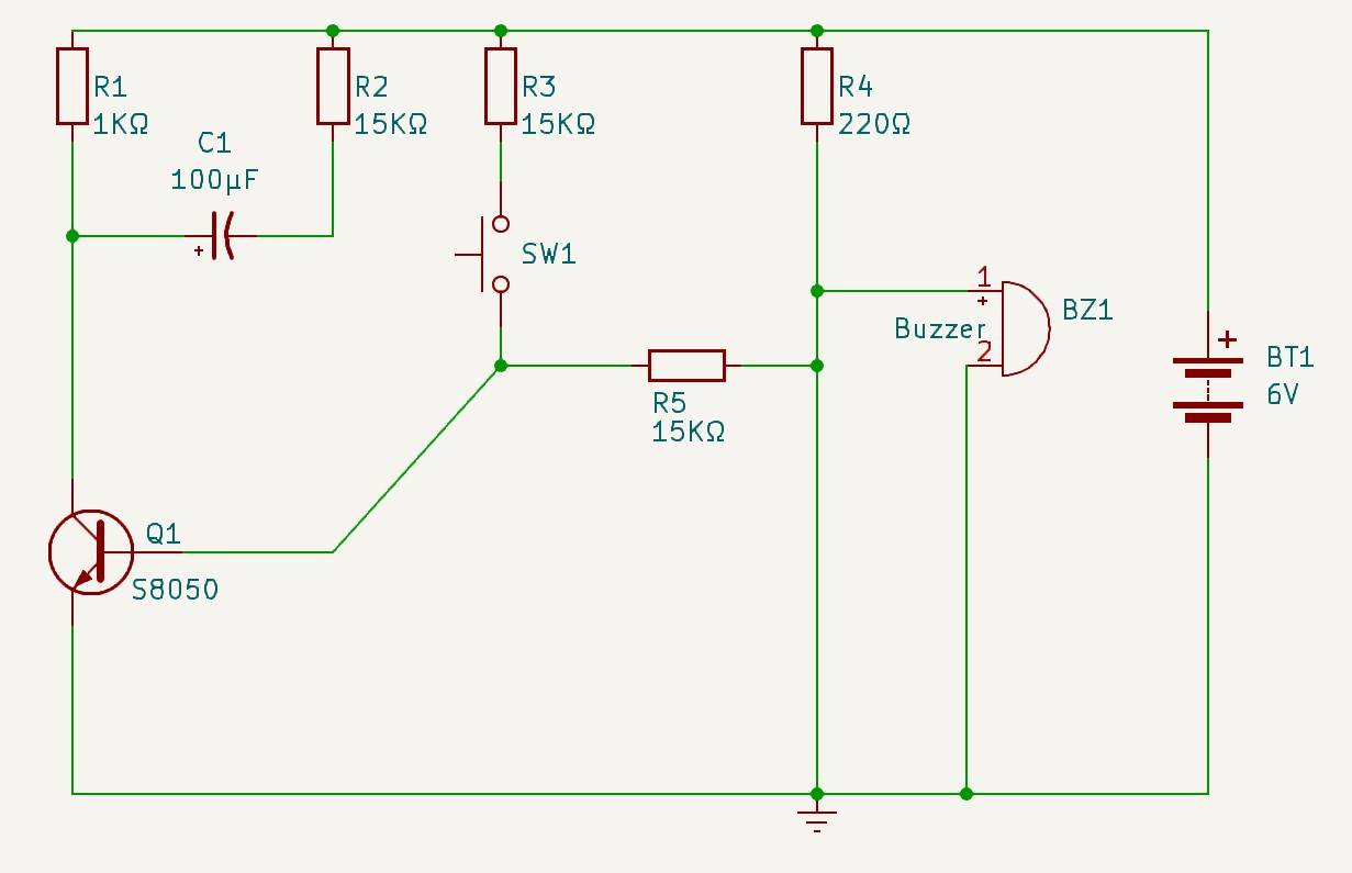 Fig.2
Fig.2Looking at this equivalent circuit diagram, we can see that the stable state of the circuit is to output low level. The buzzer is essentially short-circuited and remains in a mute state, with transistor Q1 in a cut-off state. This means that without an external trigger as input, the buzzer of the circuit will not sound because transistor Q2 will always be in a conductive state. When you press switch SW1 with your finger, it’s like introducing an external trigger to the circuit. A voltage will be generated at the left end of resistor R5, which will bring the base of transistor Q1 to a saturation state, thereby making Q1 conductive. The equivalent circuit at this time is as follows:
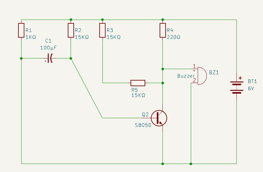 Fig.3
Fig.3As shown in Fig 3, when the switch SW1 is pressed, the base voltage of Q1 reaches 0.7V, causing Q1 to turn on, Q1 collector-emitter acts as a short circuit. This forward-biases the base-emitter junction of Q2, fixing the voltage of the right-hand plate of C1 at 0.7V and preventing it from rising. The voltage of the left-hand positive plate of C1 will drop to near 0V. If this voltage drops suddenly, a current surge in the opposite direction to the charging current will flow through the capacitor. This is caused by the discharge of stored energy back into the circuit in an attempt to maintain the voltage difference across its plates. At this point, the end of the capacitor connected to the base of transistor Q2 will generate a negative voltage, causing Q2 to cut off. The equivalent circuit at this time is as shown below:
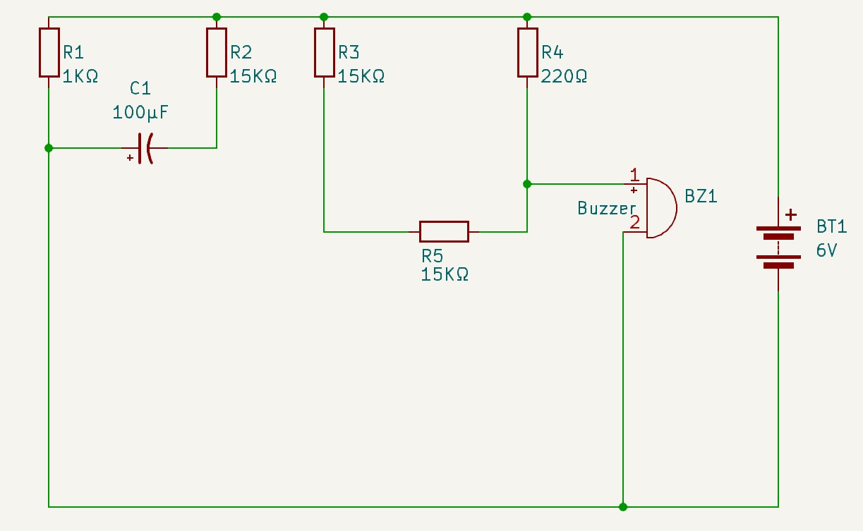 Fig.4
Fig.4
At this point, the circuit outputs a high level, causing the buzzer to sound. However, the buzzer won’t continue to sound indefinitely. This is because the circuit contains a momentary pushbutton switch . Once the button is released, the switch immediately opens. The reason the buzzer can sound at this point is due to the time it takes for the power supply to charge the capacitor. This charging time is directly proportional to the product of the resistance R and the capacitance C, with the time constant τ = R.C. When the base voltage of the NPN transistor reaches 0.7V, the transistor turns on. In this circuit, the time constant τ = R.C corresponds to a voltage of 63.2% x 6V ≈ 3.8V. When the switch SW1 is pressed, the negative voltage generated at the right-hand negative plate of the capacitor C1 connected to the base of Q2 is greater than 3.8V. Therefore, after releasing the switch SW1, the power supply needs to charge the capacitor for a time equal to one RC constant before the base of Q2 can reach the saturation voltage of 0.7V. Before the voltage at the right-hand plate of the capacitor connected to Q2 reaches 0.7V, the circuit output is high level and the buzzer will sound. Once it reaches 0.7V, the transistor Q2 turns on, the circuit outputs a low level, and the buzzer no longer sounds. Therefore, in this circuit, the high level output of the circuit is a transient state.
In summary, in this circuit, we consider the low-level output of the circuit as the steady state, and the high-level output as the transient state. The circuit only enters the transient state(unstable state) when an external trigger occurs, such as pressing a switch. The duration of this transient state is determined by the time constant of the RC coupled circuit.
The content above presents a practical circuit that uses a momentary pushbutton switch in conjunction with a buzzer. This setup allows you to intuitively experience the workings of a monostable multivibrator circuit through the sound produced by the buzzer. However, a monostable multivibrator circuit is typically used in scenarios where there is an input signal. To deepen your understanding of this, we will explore a theoretical circuit next. Please note that this is a theoretical circuit. If you were to build this circuit in the real world using the component parameters provided, it might not function as expected because it’s an idealized circuit. In reality, you would need to consider factors such as component tolerances, temperature, and interference from power and signal sources. Therefore, if you plan to build this circuit in the real world, you would need to conduct multiple experiments and make adjustments to achieve the desired results.
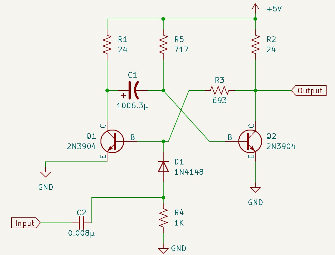 Fig.5
Fig.5Fig.5 presents a collector-coupled transistor Monostable Multivibrator circuit. Let’s delve into how it operates:
When the 5V DC power is applied, the base of transistor Q2 is connected to Vcc via the biasing resistor R5, which leads Q2 to turn ON. Q2 operates in the saturation state and its collector – emitter acts as a short circuit. The base of Q1 is connected to the ground by R3, causing Q1 to turn OFF and operate in the cut-off state, and its collector – emitter acts as an open circuit. This represents that the circuit's "Stable State" has zero output (LOW level output).
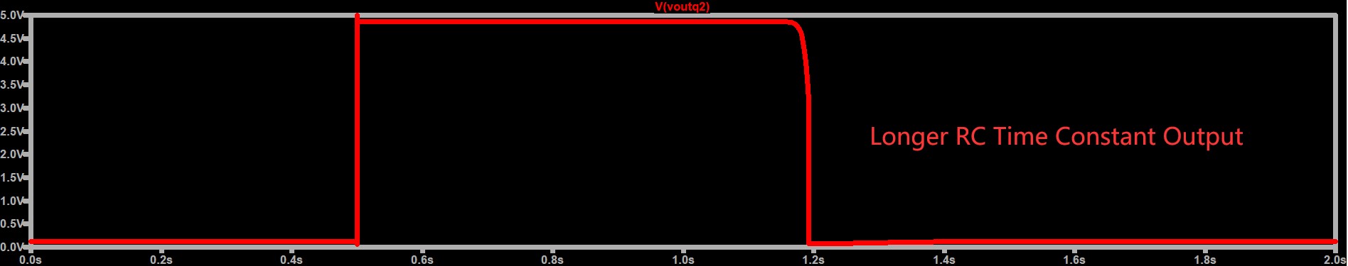
If now we apply a positive pulse to the input port, the fast-rising edge of the pulse will pass through capacitor C2 to the base of Q1 via the blocking diode and turn Q1 ON. Q1 operates in the saturation state and its collector – emitter acts as a short circuit. During this process, the C1 left-hand positive plate voltage drops down from 5V to almost 0V, as we know the capacitor has a characteristic that it prevents sudden voltage changes across their terminals, so the C1 right-hand negative plate voltage will be changed quickly to -0.693x5V≈-3.5V. This action results in transistor Q2 now having a minus base voltage(around -3.5V) and turns it OFF. This represents the circuit second state, the "Unstable State" with an output voltage equal to Vcc.
However, the Unstable State doesn’t persist for long. The timing capacitor C1 begins to discharge the -3.5V through the timing resistor R5, aiming to charge up to 0.7V(Some beginners might be confused and ask: ‘The voltage is clearly increasing, so why do we say it’s discharging instead of charging? The term “discharge” in this context is a bit counter-intuitive. When we say that the capacitor C1 is discharging, we mean that it is losing the charge it initially had). This negative voltage at the base of transistor Q2 gradually decreases at a rate determined by the time constant of the R5 and C1 combination. Once the right-hand plate of C1 charges up to 0.7V, the base of Q2 operates in the saturation state and its collector-emitter junction acts as a short circuit. This causes Q1 to switch off again, and the monostable multivibrator automatically reverts back to its original stable state, ready for the next positive trigger pulse to restart the process.
Monostable Multivibrator Waveforms

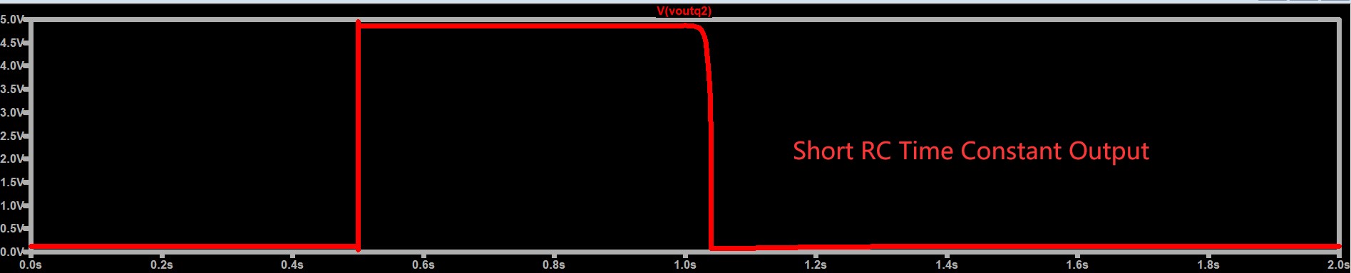
We can see from the above waveforms that the width of the output pulse can be changed by the RC time constant by adjusting the capacitor C1 , resistor R5 or both. You can use this feature to produce a time delay within a circuit with the same frequency of the input trigger pulse signal.
How to Design a Monostable Multivibrator Circuit?
R1, R2 – Collector Resistor
Collector Resistor R1 and R2 should be calculated depending upon the collector current requirement, the equation is below:
R5 – Q2 Base Resistor and Timing Resistor
The resistor R5 should be selected such that it ensures adequate collector current to transistor Q2 when it is in saturation.
-
The minimum base current, denoted as Ibmin, is calculated by dividing the collector current, Ic, by the transistor's forward current transfer ratio, commonly known as hFE or β:
-
The safe base current, denoted as Ib, is calculated as three times the minimum base current, or Ibmin. This can also be expressed as three times the ratio of the collector current, Ic, to the transistor’s forward current transfer ratio, β:
R3 – Q1 Base Resistor
The resistor R3 should be selected such that it ensures adequate collector current to transistor Q1 when it is in saturation:
C1 – Timing Capacitor
As
So,
R4, C2 – Differentiator
Capacitor C2 in conjunction with Resistor R4 constitutes a differentiator circuit, designed to generate sharp trigger pulses for the base of transistor Q1. The diode D1, acting as a unidirectional conductive path, permits only positive pulses to reach the Q1 base:
, where Tmin is the lowest time period of the signal that should be differentiated.
The differentiator waveform looks like below:
Monostable Multivibrator Circuit Calculator
Seconds
V
V
V
mA
Ω
Hz
Creative Commons tutorials are CC BY-SA 4.0 License
1 Comment(s)
Filipe
Mar 11, 2024 17:53
Extremely detailed article! It helps me understand how the monostable multivibrator works and saves me lots of time on my homework!Thanks