Bipolar Junction Transistor
April 09, 2024
Bipolar Junction Transistor
This tutorial is a deep dive into BJT transistors and will guide you through everything you need to know about them, all in one place. A Bipolar Junction Transistor (BJT) is an active device or active component. Active devices require a power source (such as a battery) to exhibit their characteristics and are generally used for signal amplification, transformation, etc. On the other hand, passive devices can exhibit their characteristics without a power source, such as resistors, capacitors, and inductors.
The primary functionalities of a Bipolar Junction Transistor (BJT) are its amplification and switching capabilities. This article primarily elaborates on these two functionalities, aiming to assist beginners in comprehending the characteristics of a BJT transistor.
Why We Call Bipolar Junction Transistor 'NPN' or 'PNP'?
All Bipolar Junction Transistors (BJTs) are classified into two types based on the doping of their regions: NPN or PNP, the categorization of BJT transistors into NPN and PNP depends on the structure and not the material itself even though transistors were made from germanium but most modern BJTs are made from silicon.
Let's use the NPN transistor as an example to explain everything about BJT transistors.
 Fig.1
Fig.1
In image Fig.1 we can see that a real S8050 NPN transistor has three pins, the No.1 pin is the collector, the No.2 pin is Base, the No.3 pin is the Emitter. A transistor is named 'NPN' or 'PNP' based on the arrangement of the N-type and P-type semiconductors in its structure. In an NPN transistor, the emitter and collector are made of N-type semiconductor material, which has an abundance of free electrons, while the base is made of P-type semiconductor material, which has an abundance of holes. The names 'NPN' and 'PNP' describe this arrangement of semiconductor materials, not the roles of the collector, base, and emitter in the transistor's operation. The terms 'collector', 'base', and 'emitter' refer to the three terminals of the transistor and their roles in its operation. The collector collects the current carried by the electrons (in an NPN transistor) or holes (in a PNP transistor), the base controls the current flow between the emitter and collector, and the emitter emits the charge carriers (either electrons or holes).
So, an N-type semiconductor is so named because it has an abundance of free electrons, these electrons are negatively charged, hence the 'N' for negative. A P-type semiconductor, on the other hand, has an abundance of 'holes', these holes are considered to carry a positive charge, hence the 'P' for positive. So, an NPN transistor is named for its arrangement of N-type and P-type semiconductors. It has an N-type semiconductor on both ends (the emitter and collector), and a P-type semiconductor in the middle (the base). Hence, it is named NPN, which can be thought of as an abbreviation for Negative-Positive-Negative.
Why Do BJT Transistors Conduct Electricity?
Fig.2 illustrates the cross-section of a real NPN transistor. The red bands between the emitter, base, and collector represent two distinct PN junctions that naturally form when no power source is applied. These PN junctions are also known as depletion regions, which simultaneously act as insulating layers. In the absence of an external voltage, the lower part of the image represents the movement of particles in a PN junction. In this state, some holes from the P-type semiconductor are attracted to the N-type semiconductor, and some electrons from the N-type semiconductor are attracted to the P-type semiconductor. This movement of charge carriers leads to the formation of a 'depletion region' in the middle. The depletion region acts as an insulating barrier and creates an electric field. The system reaches a state of equilibrium when no further net movement of charge carriers occurs.
So, when no external power source is applied to a NPN Bipolar Junction Transistor, its equivalent diagram is as shown in Fig.3:
Now look at the following image, Fig.4
When there is a reverse-biased voltage applied to collector and base, as we know that in a p-n junction, the p-region has a high concentration of holes (positive charges), and the n-region has a high concentration of electrons (negative charges). When the p-n junction is in equilibrium, these charge carriers move from the high concentration region to the low concentration region through a mechanism called diffusion, forming a depletion region. This depletion region is a region devoid of charge carriers, and it acts as a barrier to current flow. When we apply a reverse bias (i.e., connect the p-region to the negative terminal of the power supply and the n-region to the positive terminal), the external electric field is in the same direction as the internal electric field, this combined effect causes the depletion region to widen. This is because two electric fields in the same direction superimpose, a stronger electric field will appear, this stronger electric field will make the original depletion region become wider. Therefore, a reverse bias causes the depletion region to become thicker, the larger the reverse bias voltage, the thicker the depletion region becomes.
When understanding Fig.4, some students might question the behavior of a p-n junction under reverse bias. In equilibrium, there are a few electrons in the p-region and a few holes in the n-region. When a reverse-bias voltage is applied to the p-n junction, with the negative terminal of the voltage source connected to the p-region and the positive terminal connected to the n-region, wouldn't the negative terminal push the few electrons in the p-region back to the n-region? Similarly, wouldn't the positive terminal push the few holes in the n-region back to the p-region? Wouldn't this cause the depletion region of the p-n junction to become thinner? Why does it instead become thicker?
Well, they're right to be curious about the above topic! There seems to be a slight misconception about the mobile charge carriers present in a p-n junction at equilibrium. In a p-n junction at equilibrium, there are indeed some minority carriers present in both regions. There will be a small number of electrons in the p-region and a small number of holes in the n-region. However, the majority carriers (holes in p and electrons in n) are the ones that dominate the diffusion process. They move from their high concentration region to the low concentration region. This diffusion creates an internal electric field that opposes further diffusion, eventually reaching an equilibrium state. When a reverse bias is applied, the negative terminal is connected to the p-region and the positive terminal to the n-region. This external electric field does push the already existing minority carriers (electrons in p and holes in n) further away from the junction. However, the crucial point is that the main effect of the reverse bias is on the majority carriers. The stronger electric field due to reverse bias forces the majority carriers (holes in p and electrons in n) away from the junction to a much larger extent than the minority carriers were pushed before. This depletion of majority carriers from both sides widens the depletion region significantly.
So, when only a reverse-biased voltage is applied to the base-emitter junction, no current will flow through the NPN Bipolar Junction Transistor.
But, what will happen if we apply a forward-biased voltage to the emitter-base junction? The illustration is shown below:
In Fig.5, a small voltage (approximately 0.7V) is applied to the circuit, creating a forward bias in the emitter-base junction. This will overcome the potential barrier of the depletion region in the emitter junction. Under the influence of this forward bias voltage, the depletion region of the emitter-base PN junction becomes thinner. This allows the majority carriers (in this case, electrons from the N-region of the emitter) to diffuse into the base. As we know, the emitter of an NPN transistor, which is made of N-type material, is usually doped more heavily than the collector. This means there are more free electrons in the emitter region. When a forward-biased voltage of 0.7V is applied to the emitter-base junction, the external electric field pushes the electrons from the emitter to the base. Only a small number of these electrons recombine with the holes in the base region. The remaining free electrons continue to flow through the base to the collector. This is why the heavily doped region is named the 'Emitter' - its primary function is to emit free electrons. The collector's job is to collect these free electrons. Hence the less heavily doped region is named the 'Collector'.
The base region of a transistor is designed to be very thin primarily to minimize recombination of electrons and holes. In an NPN transistor, when electrons are emitted from the emitter to the base, we want as many electrons as possible to pass through the base to the collector. If the base region is too thick, more electrons will recombine with holes in the base, reducing the number of electrons reaching the collector and thereby decreasing the transistor's amplification effect. Therefore, to enhance the performance of the transistor, the base region is typically designed to be very thin. The illustration is shown below:
In Fig.6, we can see that the direction of the conventional current is from the collector to the base and then to the emitter. It's important to note that when we refer to 'current', we're actually referring to 'conventional current' which is just a concept used in electrical engineering and physics to describe the direction of positive charge flow, which is opposite to the direction of electron flow. Electrons, which are real particles, flow in the opposite direction.
One Function of BJT Transistors - Utilization as a Switch
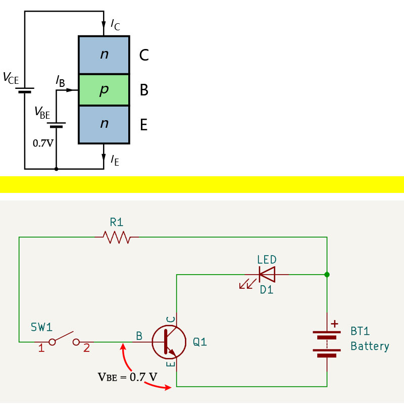 Fig.7
Fig.7
As shown in Fig.7, When a forward-biased voltage of 0.7V DC is applied to the emitter-base junction of an NPN transistor, it causes electrons from the heavily doped emitter region to flow through the base region to the collector region. This puts the transistor in a state of conduction. The direction of current is opposite to the flow of electrons, i.e., it flows from the collector to the base and then to the emitter region. This 0.7V is known as the 'base-emitter junction voltage'. Some BJT transistors have this voltage at 0.6V. For specifics, refer to the datasheet provided by the transistor manufacturer. In such situation, the Bipolar Junction Transistor acts like a switch. When the forward-biased voltage between the emitter and base is less than 0.7V, the externally applied voltage doesn't generate a strong enough electric field to push the electrons from the heavily doped emitter region across the depletion region to the collector region. Therefore, when the forward-biased voltage between the emitter and base is less than 0.7V, the transistor is in a cut-off state, equivalent to an open switch
Another Function of the BJT Transistor - Signal Amplifier
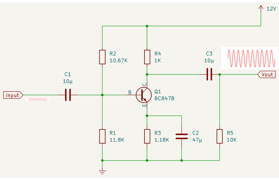 Fig.8
Fig.8
In Fig.8, the NPN transistor serves as an amplifier. Some students mistakenly believe that transistor amplifier circuits merely multiply the input signal at the base by the transistor's current gain factor (β). However, this understanding is incomplete. Directly amplifying the input signal through the transistor won't yield the desired output because input signals are often very weak. Even the peak value of the input signal may not turn the transistor on. Therefore, when designing an amplifier circuit with an NPN transistor, it's essential to include a biasing circuit at the base to ensure the transistor operates in the active region. A biasing circuit provides a constant voltage to the base of the transistor. This voltage sets the transistor's operating point in the active region.
In essence, transistor amplification occurs by applying a small input signal to the base bias circuit. This variation in base current then propagates to the collector. Therefore, transistor amplification involves controlling a large current using a small, variable current. If the input signal remains constant, the transistor remains functional but no longer amplifies varying signals. In other words, when the input signal is constant, the transistor's output also remains constant. Thus, we cannot observe transistor amplification when the input signal is a constant current.
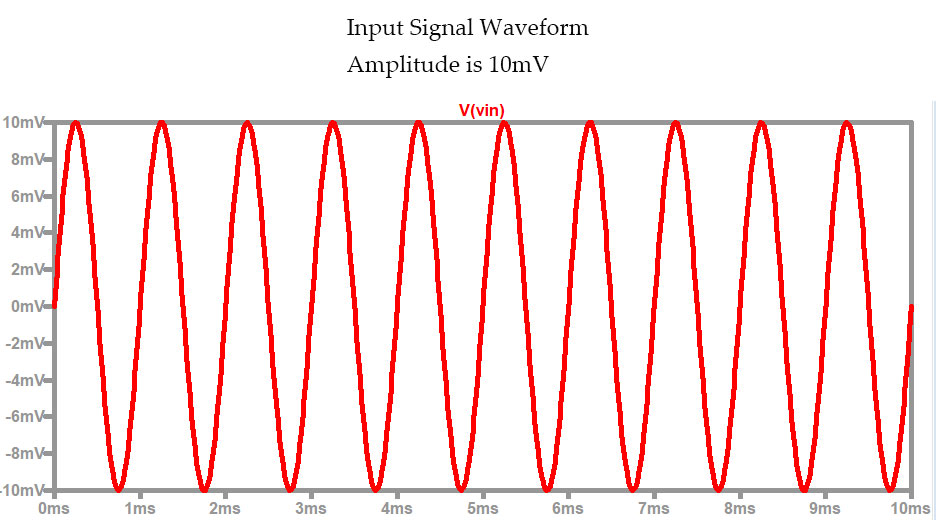 Fig.9
Fig.9
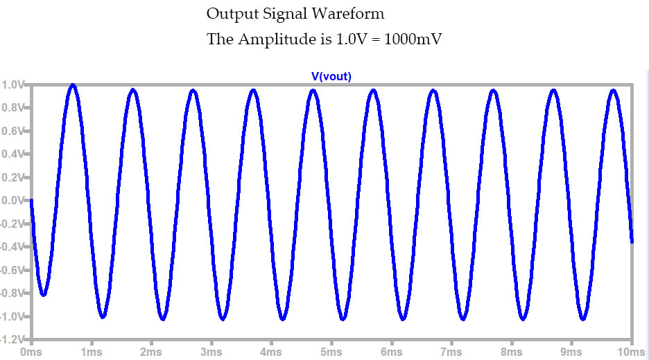 Fig.10
The Fig.8 is the example circuit of common-emitter configuration (CC), the R1 and R3 are the Biasing resistors, R2 is the load resistor for base, C1 is the Coupling capacitor, C2 and C3 are the Bypass capacitors.
- Biasing resistors (R1, R3) set the base voltage of the transistor (Q1), which in turn determines the amount of current flowing through it and establishes the operating point for the amplifier circuit. The specific values chosen for these resistors depend on the transistor characteristics and desired gain of the amplifier.
- Feedback resistor (R2), is used in conjunction with R1 to form a voltage divider, providing a stable bias voltage for the transistor's base.
- R5 could be part of the output stage, helping to set the gain of the amplifier or stabilize the output signal
- Coupling capacitor (C1) blocks any DC bias voltage from the previous stage while allowing the AC signal to pass to the base of the transistor. This prevents unwanted DC offsets from being amplified.
- Bypass capacitors (C2, C3) provide an AC ground path for the power supply pins of the transistor (Q1). They help to reduce noise and improve the stability of the circuit by filtering out unwanted AC signals on the power supply lines.
Fig.9 is the input signal waveform, its amplitude is 10mV; Fig.10 is the output waveform, its amplitude is 1V=1000mV. From this, we can observe that the example amplifier circuit amplifies the input signal by a factor of 100.
Why can a BJT (Bipolar Junction Transistor) amplify signals, while diodes, resistors, and capacitors cannot?
Somebody may feel puzzled while learning about transistors, wondering why transistors can amplify signals while other electronic components lack this property. To answer this question, we need to start with the material and structure of transistors mentioned earlier. From the content above, we already know that the emitter region of an NPN transistor is more heavily doped than the collector region, resulting in a higher density of free electrons in the emitter compared to the collector. Consequently, even a small change in base current leads to a tiny forward-biased voltage across the emitter-base junction. This voltage creates a small external electric field, causing a flow of electrons (in a ratio of β) from the emitter to the collector. This phenomenon is the reason why transistors exhibit signal amplification. Even though diodes are also semiconductor devices composed of two layers (p-n junctions). Unlike transistors, diodes do not have the three distinct regions (emitter, collector, and base). Instead, diodes have only two terminals that are made of p-type and n-type semiconductor materials but lack the specific regions found in transistors that they only allow current flow in one direction (from the anode to the cathode) when forward-biased; when reverse-biased, it block current flow. However, diodes do not actively amplify signals; they act as rectifiers or voltage regulators.
Resistors are passive components that limit current flow without amplification; they consist of materials with fixed resistance values and do not actively magnify signals, unlike transistors, resistors lack the specific p-type and n-type semiconductor regions necessary for signal amplification. Capacitors store and release energy but do not inherently amplify signals, their primary function is to store charge and provide filtering or timing functions. Capacitors store and release energy, primarily serving as charge reservoirs for filtering and timing purposes. However, unlike transistors, capacitors lack the necessary structure for active signal amplification. That's why only Bipolar Junction Transistors can amplify signals, while capacitors, resistors, and diodes cannot.
Input Characteristics Curves of a Typical Bipolar Transistor
Input characteristics of a transistor are curves showing the variation of input (base) current IB as a function of input (base-emitter) voltage VBE, when the output (collector-emitter) voltage VCE is kept constant that is one of the most two crucial curves of the BJT transistor, the other is output characteristics curve. The input characteristic curve serves as a critical tool in understanding transistor behavior, illustrating the ease with which the transistor can be activated (forward biased) by the base-emitter voltage. A steeper curve indicates a smaller requisite forward-biased base-emitter voltage change for a significant increase in base current. Furthermore, this understanding aids in the selection of appropriate biasing conditions, evaluation of linearity and distortion, determination of key parameters, and troubleshooting of circuit issues. It offers invaluable insights that facilitate the design, analysis, and optimization of transistor-based electronic circuits. That is why sometimes but not always we need to read the input characteristic curves when we using a specific BJT transistor. because most BJT transistors of a particular type (e.g., S8050 etc.) will have very similar input characteristic curves. Manufacturers ensure consistency within a specific model. The transistor's datasheet provides crucial information about its typical behavior, including the expected range for base current (IB) versus base-emitter voltage (VBE). This eliminates the need for individual curve plotting. The primary concern is identifying the active region for amplification. Datasheets and knowledge of typical BJT behavior can guide you towards this region without a specific curve. But, when dealing with high-precision circuits, you may need to determine their input characteristic curve based on your practical circuit. Consider factors such as environmental temperature-induced drift, potential impedance, and other relevant parameters. This task can be complex, requiring a comprehensive analysis of multiple factors to ensure the accuracy and stability of the circuit.
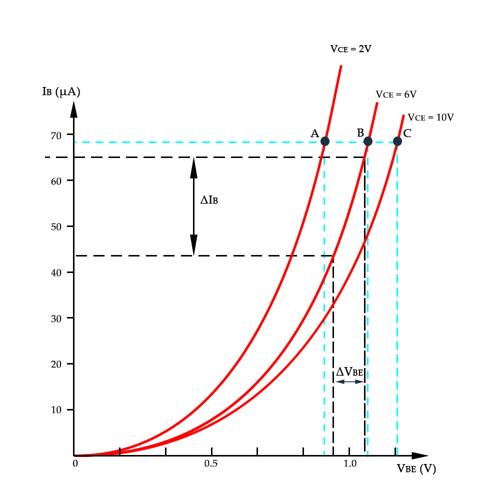 Fig.11
As shown in Fig.11, the three curves correspond to three different constants, which are VCE=2V, VCE=6V, VCE=10V, respectively. We can find that as the value of the horizontal axis VBE increases, the increment of the vertical axis IB also becomes larger. This means that after entering the active region of the transistor, a slight change in VBE will cause a significant change in IB. Therefore, we find in this coordinate graph that the curve of VCE becomes steeper as VBE increases.
From the Fig.11, we also find that with the increase of VCE (it should be noted that VCE is constant in this coordinate graph, and different curves correspond to different values of VCE), to generate the same base current IB, a higher VBE bias is required. Some students may wonder why it needs more VBE to generate same amount of current for a larger VCE. Here we will give you the answer by analyzing the BJT NPN transistor inner structure and electrons moving trend while applying different DC voltage to the collector region.
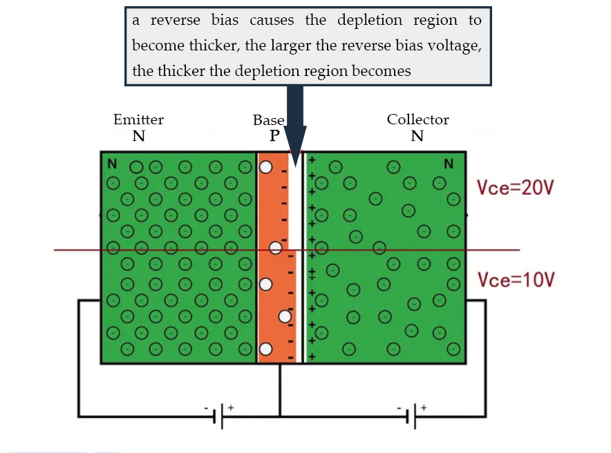 Fig.12
As shown in Fig.12, when reverse-biased voltage applied to the collector-base junction, there will be a gap(depletion region) generated between the p-region and n-region, the case of VCE=20V is more wider than the case of VCE=10V (if you forget why would this happen please go to the explanation of Fig.4). So, when the VCE increases, in order to generate the same amount of base current to flow through the base-collector junction, a larger VBE is required to apply to the base region to conquer the larger gap(depletion region) between the collector-base p-n junction.
Output Characteristics Curves of a Typical Bipolar Transistor
Output characteristics of a transistor are curves showing the variation of the output current IC as a function of output voltage VCE, when the input current IB is kept constant.
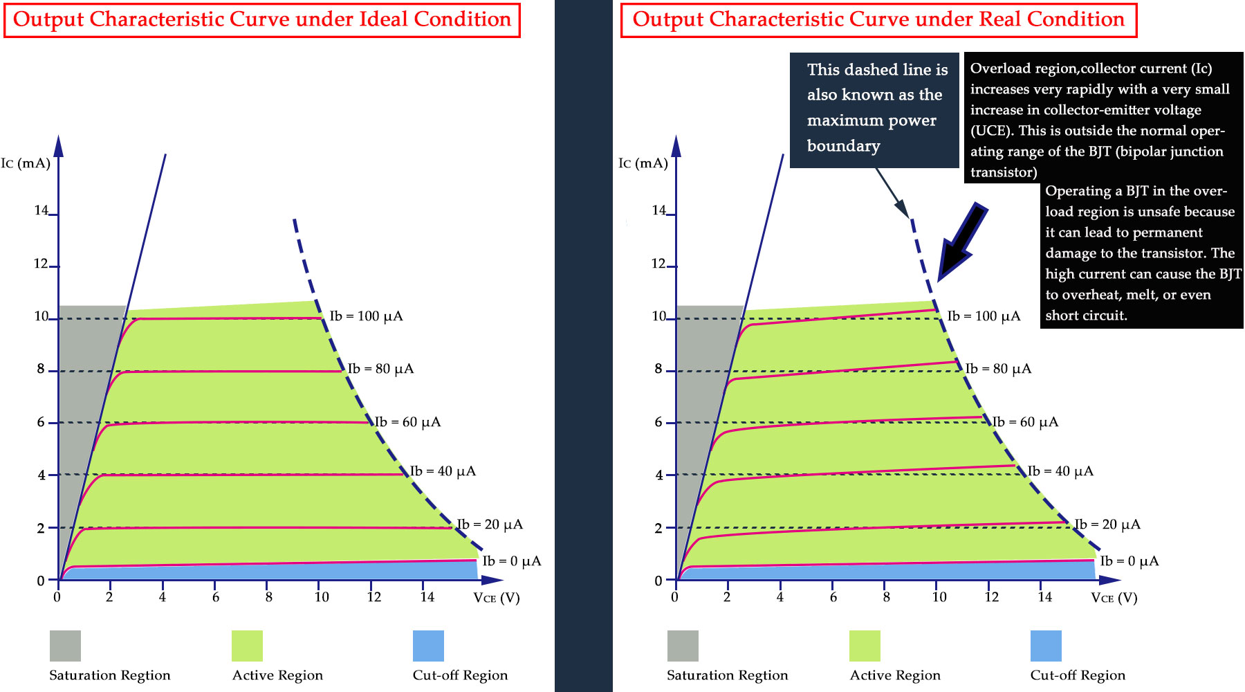 Fig.13
As shown in Fig.13, the output characteristic chart contains a set of curves, each corresponding to a different constant, IB. The left side is the ideal condition, you can see that in the active region, for specific curve of the constant of IB, even though the VCE increases, the IC remains the same, because in active region, IC=β.IB, the IC has nothing to do with VCE on the premise of that the IB kept constant. However, in the real world, the curves of constant IB in the active region have a slightly rising straight lines (while in the ideal condition of the active region, the slope equals 0, forming a horizontal line), whatever the value of VCE it is. This is because while the collector current is primarily controlled by the base current, there's a small increase in IC with increasing VCE due to the Early Effect. This effect arises from the widening of the depletion region in the collector-base junction as the voltage increases.
why Early Effect happened?
As we learned from the Fig.12, a reverse-biased voltage applied to the collector-base junction widens the depletion region between the collector and base. At the same time, this widening effectively reduces the base width (the region where collector and emitter currents interact) that a narrower base width allows a greater proportion of the emitter current (IE) to flow directly to the collector as collector current (IC), instead of recombining in the base region. This phenomenon causes a slight increase in IC with increasing Vce for a constant base current (IB).
The Early effect can be described by a parameter called the Early voltage (Va). The relationship between collector current (IC), base current (IB), collector-emitter voltage (VCE), and Early voltage (Va) can be expressed using the following formula:
- IC is the collector current
- β is the current gain factor, also known as the base current amplification coefficient
- IB is the base current
- VCE is the voltage between the collector and emitter
- Va is the Early voltage, also known as the base-collector voltage
The '+ (VCE / Va)' leads to a slightly rising straight lines in the active region.
Determine the Q-point
The Q point, also known as the operating point, bias point, or quiescent point, is an extremely important point for a specific amplification circuit composed of NPN transistors. The Q-point is not only related to the characteristics of the transistor itself, but also related to the bias circuit around the transistor.
The reason for setting a static operating point is to ensure that the output waveform of the transistor amplifier circuit does not distort. As we learned earlier in this article, the input signal alone cannot directly amplify the transistor because the current and voltage of the input signal are too weak and cannot drive the transistor to work. It is only after the input signal is superimposed on the bias circuit of the transistor that the transistor can amplify the input signal. This bias circuit, which is also the circuit when the transistor is operating in a static state, and the static operating point we mentioned, is a certain point on the output characteristic curve of the transistor. Once this point is determined correctly, it is equivalent to determining the bias circuit of the transistor. If this bias circuit is used to work with the transistor, the output waveform will not be cut off or saturated. This static operating point can make the output end of the transistor get a complete waveform that is a specific multiple of the input waveform, possibly with a phase shift.
To help you better understand how to set the Q point, we have drawn the below simplified circuit diagram for you.
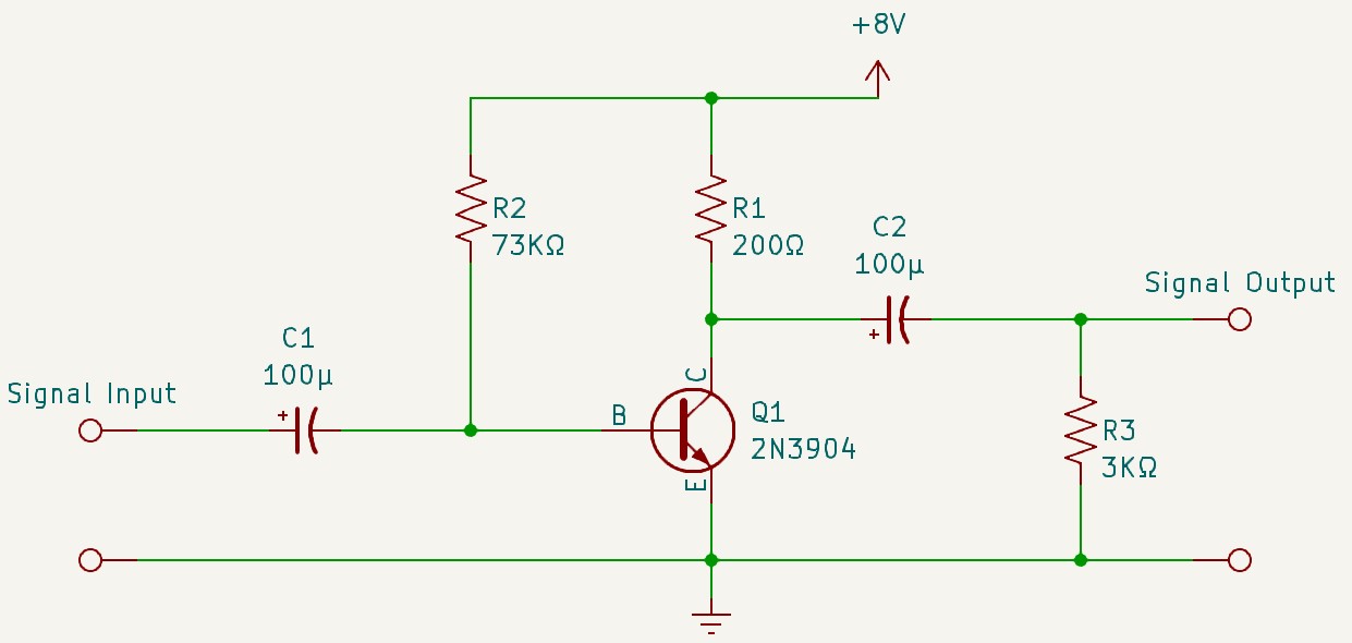 Fig.14
Below Fig.15 is the 2N3904 NPN transistor's output characteristic curves
In the amplification state of an NPN Bipolar Junction Transistor (BJT), the emitter junction is forward biased and the collector junction is reverse biased. Assuming the emitter voltage is 0V, according to the datasheet, 2N3904 is an NPN transistor, the conduction voltage is about 0.7V. In Fig.14, The base resistance R1 is adjusted to make the base voltage around 0.7V. At this time, the resistance of R2 is 310KΩ. The collector resistance R1 is 200Ω. The base voltage VB is 0.7V, and the collector voltage Vc is 7.22V. Since VC>VB>VE, the transistor is in the amplification state. The base current Ib at this time is 24μA (got this value by the ammeter). Although selecting a base current (IB) of 24μA allows the Q1 transistor to enter the amplification state, it is observed from Fig.15 that this value of IB is too low on the characteristic curve (the minimum IB value on the curve is 50μA). This could potentially lead to 'cutoff distortion (Clipping Distortion)' in the circuit. Therefore, it is necessary to readjust the circuit to ensure that the base current IB corresponds to the most suitable curve within the active region. Prior to determining this curve, it is essential to plot the Load Line.
Before we set the Q-point, we need to know about the Load Line which describes all possible states of the transistor under a given supply voltage and load resistance. This line connects two extreme operating states of the transistor: saturation and cutoff. In Saturation State, the transistor is on, the collector current is at its maximum, and the collector voltage is close to 0. In Cut-off State, the transistor is off, the collector current is close to 0, and the collector voltage is at its maximum.
Applying Kirchhoff's voltage law to the circuit in Fig.14, we get VCE=VCC-IC.RC. With IC=0, VCE equals the supply voltage VCC of 8V. When VCE=0V, IC is VCC/RC=0.04A. These points can be used to plot the DC load line on the output characteristic curve. In this situation, the intersection of the load line with the y-axis (IC axis) is at A point, (0,0.04), and the intersection with the x-axis (VCE axis) is at B point, (8,0). With these results, we can plot the load line on the output characteristic curves like below:
In Fig.16, we can see that the Q points for different constant IB are on the lines between the A and B, i.e., Q1 to Q5.
Now, we've plotted the load line for this output characteristic curves, and we found that the base current (IB) of 24μA we calculated before was too low on the characteristic curve. Thus, we need to find a Q point on this load line to serve as the optimal static operating point for this circuit. One principle we adhere to when seeking the static operating point is that it is generally appropriate to set the static operating point to the center of the DC load line. This is because at the center of the load line, the amplifier has the maximum dynamic range for changes in the input signal, i.e., it can handle the maximum amplitude of the input signal without distortion. From Fig.16, we find that point Q4 is closest to the center of the load line. Therefore, we decide to choose Q4 as the Q point for this circuit. Q4 is also on the curve of constant IB=100μA. Thus, we need to adjust the base resistance R2 to 73kΩ, raising the base current Ib from the original 24μA to 100μA.
The adjusted circuit diagram is as follows:
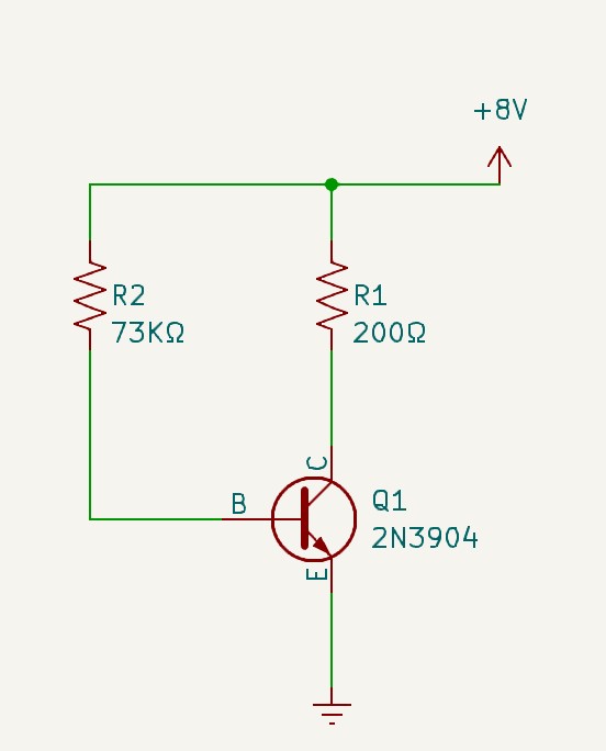 Fig.17
In Fig.17, we can see that after adjustment, the base resistance at the Q point is approximately 73KΩ. At this time, the base-emitter voltage VBE is 0.74V, the collector-emitter voltage VCE is 3.8V(as tested by voltmeter), and the base current IB is 100μA(as tested by ammeter).
We input an alternating current signal with a frequency of 500Hz and an amplitude of 10mV, as shown in Fig.18, into the circuit in Fig.17
 Fig.18
And get the output waveform like below:
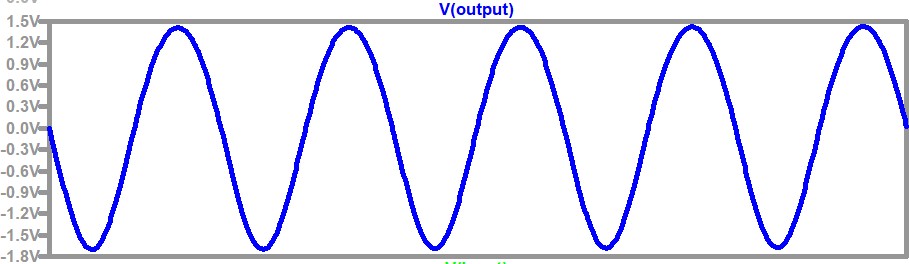 Fig.19
 Fig.19a
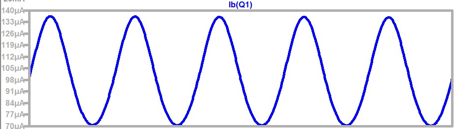 Fig.19b
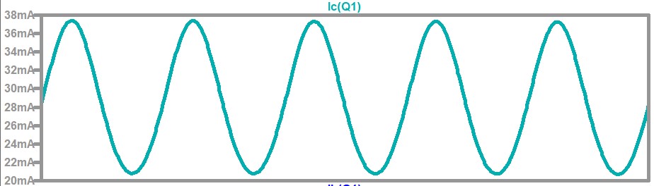 Fig.19c
From Fig.18 and Fig.19, it can be observed that the output signal is a relatively standard sine wave, with minimal distortion. The amplitude of the output signal is approximately 1.5V, which is about 150 times the amplitude of the input signal of 10mV. Fig.19a is the voltage waveform from the collector terminal (not from the right plate of C2 in Fig.14); Fig.19b is the base current waveform; Fig.19c is the collector current waveform.
The waveforms from Fig.19 to Fig.19c are incorporated into the output characteristic curves, as illustrated below:
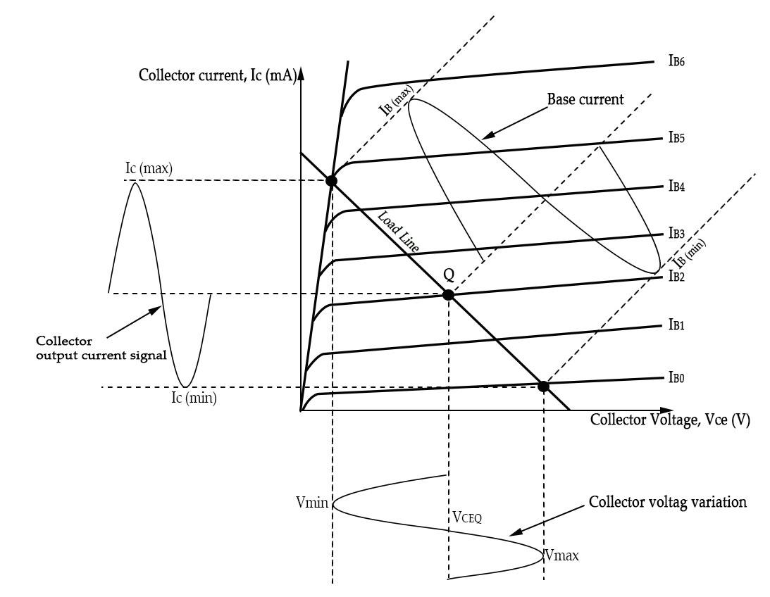 Fig.19d
In the CE configuration, a small base current is amplified to a larger current in the collector circuit. The ratio of the DC collector current IC to the DC base current IB is called the DC beta (𝛽) of the transistor:
eq.1
Typical values of 𝛽 range from 20 to 250 or higher. The 𝛽 is usually designated as hFE (current gain)in transistor datasheets. So, hFE=β
Another useful parameter in bipolar transistors is the DC alpha (𝛼). It is defined as the ratio of the DC collector current IC to the DC emitter current IE. The equation is as shown below:
eq.2
Typically, values of arange from 0.95 to 0.99, but α is always less than 1.
Through eq.1 and eq.2, we can establish a mutual conversion between α and β. That is, β can be expressed in terms of α, and vice versa. The equations representing this mutual conversion are as follows:
β is the more crucial parameter for most BJT amplifier circuits because the common-emitter configuration is dominant. When designing or analyzing a common-emitter amplifier, β tells you how efficiently the base current controls the output collector current. In general, a higher β is desirable for most BJT amplifier applications. A higher β means a smaller base current can produce a larger collector current, making the transistor more efficient in amplifying the signal. However, there are some limitations to consider with very high β transistors, such as increased susceptibility to noise and thermal runaway.
Clipping Distortion
What will happen if we increase the amplitude of the input signal from 10 mV to 100 mV and replace R1 with a 50MΩ resistor?
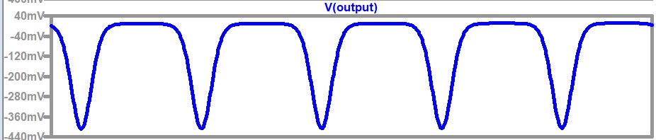 Fig.20
As illustrated in Fig.20, the lower half of the input waveform undergoes cutoff distortion result in the upper part of the output waveform undergoes cutoff distortion. This is due to the amplitude of the input signal being too high, causing the static operating point to be relatively too low. During a certain period of the negative half-cycle of the input signal, the superposition of the input signal and the static base voltage causes the voltage VBE between the base and emitter of the transistor to remain less than the turn-on voltage VON . As a result, the transistor enters the cutoff region. Therefore, the waveforms of the base current IB and the collector current IC will produce bottom distortion, i.e., the output voltage Vout waveform will produce top distortion (clipped top).
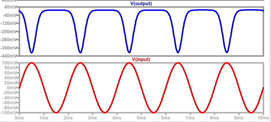 Fig.21
How to solve the Clipping Distortion Problem?
To solve the problem of clipping distortion, the static operating point needs to be adjusted again so that the voltage of Vbe is greater than 743mV under static conditions. This way, after superimposing the sinusoidal signal, Vbe can be greater than 713mV.
Since VBE = VCC - IB . RB,
if you want to increase the voltage of Vbe under static conditions, you can either reduce the base resistance RB(in this case RB is R2) or increase VCC.
Saturation Distortion
When we increase the input signal amplitude from 10mV to 30mV, the circuit enters a state of saturation distortion. The output waveform is as follows:
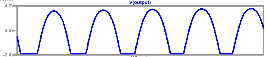 Fig.22
As shown in Fig.22, the lower half of the output waveform experiences saturation distortion. This is due to the increase in the amplitude of the input signal causing the Q point to be relatively high. During a certain period near the peak of the positive half cycle of the input signal, the transistor operating point enters the saturation region. The base current IB increases, but the collector current IC no longer increases, causing the waveform of the collector current IC to experience top distortion and the waveform of the output voltage Vout to experience bottom distortion. The input waveform and output waveform are as follows:
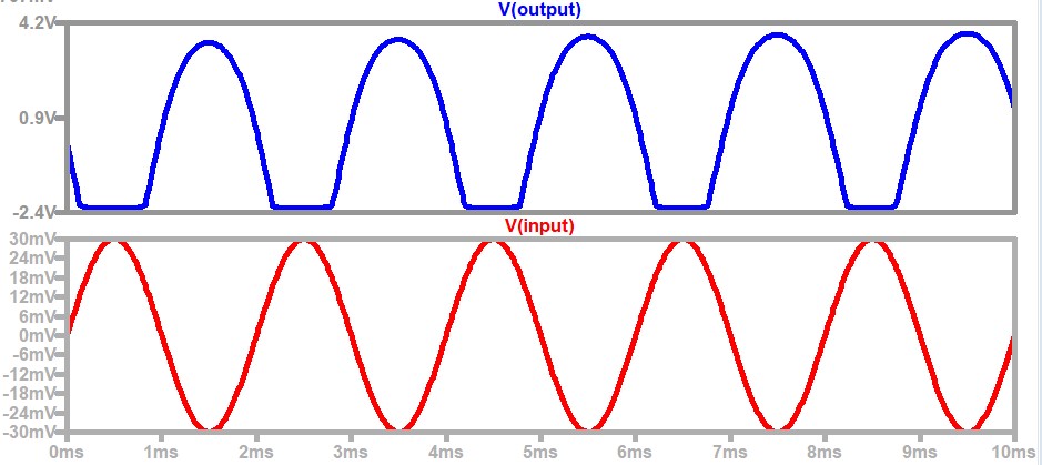 Fig.23
How to solve the Saturation Distortion Problem?
As for the solution to saturation distortion, given that VCE=VCC−β∗IB∗RC , if we want to avoid saturation distortion, we need to decrease IB , which will prevent the transistor from operating in the saturation region. One way to decrease IB is to increase RB . Alternatively, decreasing RC (in this case, it is R1) can also eliminate saturation distortion.
Can we interchange the collector and emitter?
NO!
The emitter and collector of an NPN transistor should not be reversed. Not only will reversing them destroy the transistor, but it will also significantly reduce its amplification performance. This is because when designing a transistor, the dopant concentrations in the emitter, base, and collector regions are different, following the relationship: emitter >> base > collector. Reversing the emitter and collector will result in a reduced breakdown voltage (VCEO), which is the maximum voltage that can be applied between the collector and emitter before the transistor breaks down. When reversed, the collector-base junction, which is designed to handle higher voltages, becomes the forward-biased junction. This junction has a much lower breakdown voltage compared to the collector-emitter junction, and the transistor can break down at a much lower voltage when turned 'off'. In a normal configuration, the base current controls the collector current, but when the transistor's connections are reversed, it presents lower resistance between the base and emitter, leading to an abnormally high base current that could surpass its limits and damage the transistor.
Another negative effect of reversing the connection in a bipolar junction transistor (BJT) is the decrease in hFE (current gain), a key parameter indicating the amplification of base current at the collector, which significantly reduces the transistor's amplification effect, causing it to barely conduct even with a high base current.
Below are the hFE (current gain) of normal configuration and reversed connection configuration for the collector and emitter terminals:
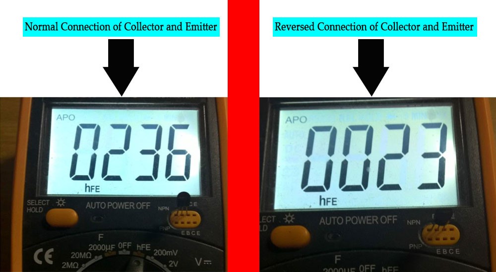 Fig.24
Fig.24 is a picture showing the amplification factor test results of an S8050 NPN transistor in both normal and reverse configurations of the emitter and collector. The left graph represents the normal configuration, while the right graph represents the reversed configuration. From these graphs, it can be observed that the amplification factor (hFE) of this NPN transistor is 236 when the emitter and collector are connected normally, and it is only 23 when connected in reverse. The reverse configuration hurts its amplification factor (hFE) significantly.
Creative Commons tutorials are CC BY-SA 4.0 License