Astable Multivibrator
February 27, 2024
Astable Multivibrator
An astable multivibrator circuit, which differs from the monostable oscillating circuit we discussed in last article, operates in a unique way. When a monostable circuit receives an external signal, it switches from a stable state to an unstable state, and then automatically reverts back to the stable state after approximately an RC (resistor-capacitor product) time period. However, the astable multivibrator circuit we are discussing in this article does not require any external signal input. It automatically alternates between two different states (high and low levels). By leveraging this characteristic, we can generate various waveforms such as square waves, sawtooth waves, triangular waves, and pulse waves at a very low cost with astable multivibrator circuit.
In order to help you better understand the working principle of a astable multivibrator circuit, we will use a simple and practically operable LED wheel flash circuit as a case study to explain it.
A Practical Example of Astable Multivibrator Circuit —— LED Wheel Flash Circuit
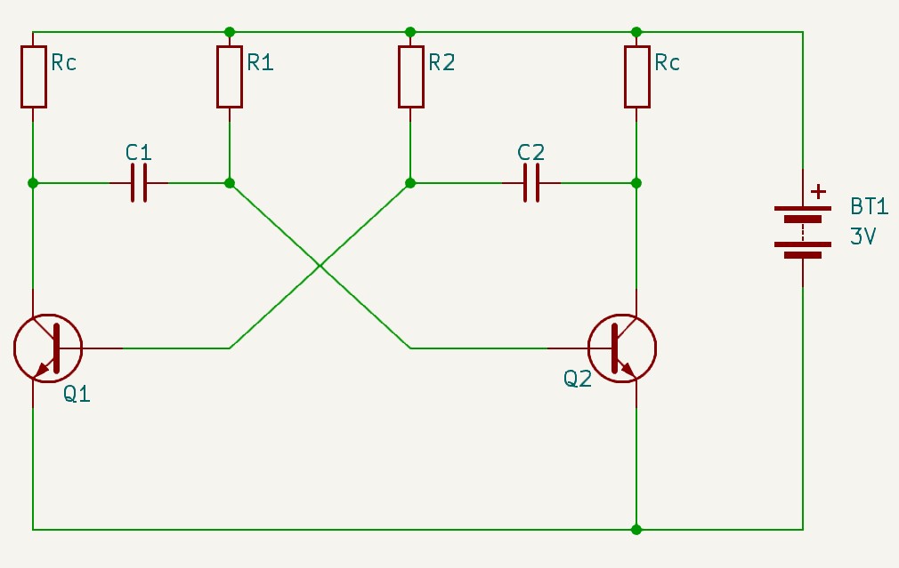
 Fig. 1
We are going to explain the detail of the working process and principle of the Astable multivibrator circuit through the simple circuit shown in Fig.1, which can actually operate. Once the circuit is connected to the power supply, it can make LED1 and LED2 flash alternately without any chip control. Its essence is to use the RC charging and discharging circuit composed of capacitor C and resistor R to create a pulse of a certain frequency to make the LED light flash.
In the real world, all resistors, capacitors, and transistors have a tolerance value. There are no two components with exactly the same value. For example, two capacitors labeled as 100μF may have slight variations in their actual values, making them unequal. This discrepancy is due to the inevitable physical and chemical changes during the manufacturing process. Similarly, even if two transistors are of the same model, such as SS9014,their parameters are not entirely identical. Even though the circuits on both sides of Q1 and Q2 in Fig.1 are symmetrical, and the values are marked as R1=R2, C1=C2, Q1=Q2, when the power is turned on, due to the different actual tolerance of each component, Q1 and Q2 will not turn on at the same time. Instead, a situation may occur where Q1 turns on first or Q2 turns on first
The specific workflow of the circuit is as follows:
When the circuit is connected to the power supply, the power supply charges the negative plate of the electrolytic capacitor through the high-value base resistors R1 and R2 simultaneously. (Some beginners may feel confused that the connection of electrolytic capacitors in the circuit has polarity requirements,the positive pole of the electrolytic capacitor should be connected to the positive pole of the battery, and the negative pole of the electrolytic capacitor should be connected to the negative pole of the battery. Their view is both right and not entirely correct. In fact, the positive terminal of an electrolytic capacitor only needs to be connected to the intended high potential end, and its negative terminal only needs to be connected to the intended low potential end. It is not required that the positive terminal must be connected to the positive terminal of the battery while the negative terminal is connected to the negative terminal of the battery)
In this circuit, the positive plate of C1 is connected to the positive pole of the power supply through the low-resistance LED1, and its negative plate is connected to the positive pole of the power supply through the high-value resistor R1. Because the resistance of LED1 is much lower than that of R1, the potential of the positive plate of C1 is much higher than that of the negative plate. Therefore, this connection method of the electrolytic capacitor in this circuit will not cause damage to the electrolytic capacitor. Since the voltage of the battery is 3V, when C1 and C2 are fully charged, the voltage of their positive plates is about 3V, and the negative plate is slightly charged, causing the voltage of the negative plate to be about 0.7V. However, due to the differences caused by the tolerance of the capacitor, resistor, and transistor, Q1 or Q2 may be turned on first. Let’s assume that Q1 is turned on first (Q2 is off), and we name this as state 1.
State 1(Q1 is ON, Q2 is OFF)
Since Q1 is in the on state, the left-hand positive plate of C1 is connected to the collector of Q1. Therefore, the left-hand positive plate of C1 is essentially connected to the ground. As a result, the voltage at the positive plate of C1 drops from 3V to almost 0V.
Due to the characteristic of a capacitor to resist sudden changes in voltage across its terminals, when the voltage at the positive plate drops abruptly from 3V to near 0V, the voltage on the negative plate will also change to around -3V to maintain the total voltage difference across the capacitor close to 3V, as C1 right-hand negative plate is connected to Q2 base, so the -3V is applied to Q2 base and keep Q2 firmly off. And then the C1 begins discharging (reverse charging) via the high-value base resistor R1. As C1 discharges, the voltage at its right plate (connected to Q2 base) becomes less negative and starts rising from -3V towards 0V, and then continue rising, until it reaches 0.7V(Some beginners may feel puzzled: even though the voltage at C1’s right-hand plate is gradually rising in this process, why it is still referred to as 'discharging'. We will explain at the final of this blog[1]), the forward-biased Q2 base-emitter junction fixes the voltage of C1 right-hand plate at 0.7 V and does not allow it to continue rising toward +3V. As the right plate of C1 is connected to the Q2 base that the 0.7V will soon turn the Q2 ON(just will, not yet ON), the state 2 is imminent. During the process of the voltage at the right plate of C1 rises to 0.7V, C2 restores its charge to the power supply voltage of 3V that prepares for the upcoming State 2.
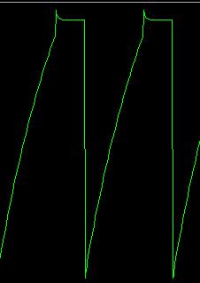
Towards the end of state1, where Q2 is in the process of turning on but hasn’t fully turned on yet, and at the same time, Q1, although conducting, is on the verge of turning off, the Q2 collector voltage begins falling that leads to the Q1 base voltage decreasing and Q1 begins cutting off, at the same time, the Q1 collector voltage begins rising, as the C1 right-hand plate is connected with the Q2 base, this change makes the Q2 conduct more. So, the initial change in input travels around the feedback loop, grows in an avalanche-like manner, until finally Q1 turns off and Q2 turns on. The waveform of the C1 right-hand negative plate (i.e. the Q2 base voltage waveform) is below:
An avalanche-like manner is evident in the voltage surge at a certain point that forms a protruding, spike-like waveform before the voltage stabilizes
State 2(Q2 is ON, Q1 is OFF)
At the end of the previous state(state 1), the right plate of the C1 reaches 0.7V, as it is connected to the base of the Q2 and Q2 switches on, the right plate of the C2 is connected to the ground by Q2. As the voltage of right plate of C2 drops abruptly from 3V to 0V, the voltage on the left plate of C2 will also change to around -3V to maintain the total voltage difference across the capacitor close to 3V. As C2 left-hand negative plate is connected to Q1 base, a maximum negative voltage (-V) is applied to Q1 base that keeps Q1 firmly off. At the meanwhile, the left negative plate of the C2 begins discharging(reverse charging) via the high-value resistor R2, the voltage at its left plate (connected to Q1 base) becomes less negative and starts rising towards 0V, and then continue rising, until it reaches 0.7V, the forward-biased Q1 base-emitter junction fixes the voltage of C2 left-hand plate at 0.7 V and does not allow it to continue rising toward +3V. As the left plate of C2 is connected to the Q1 base that the 0.7V will soon turn the Q1 ON(just will, not yet ON), the state 1 is imminent. During the process of the voltage at the left plate of C2 rises to 0.7V, C1 restores its charge to the power supply voltage of 3V that prepares for the upcoming State 1.
State 1 and State 2 continuously cycle through each other. The time interval between the two states is related to C1, C2, R1, and R2.
The total period of oscillation is given by:
frequency of oscillation is:
As
So,
Where, R is in Ω's, C is in Farads, T is in seconds and ƒ is in Hertz.
The theoretical calculation does not take into account real-world factors such as temperature, power supply stability, and parasitic capacitance or inductance, which can all affect the performance of the circuit.
How to Design a Astable Multivibrator Circuit?
Rc – Collector Resistor
Rc is used to limit the current at the collector of the transistor, ensuring that the transistor operates within a safe range. If the current exceeds the maximum that the transistor can handle, it could lead to a breakdown of the transistor.
, where V is the voltage across the resistor Rc, Ic is the current flow through the transistor collector end.
Generally, ,
But when you add a load section to the transistor emitter,
where Vload is the voltage drop across the load.
It’s important to note that when selecting components, the maximum collector current (Ic) should be significantly greater than the required current of the emitter load. This is because, in addition to acting as a switch, a transistor also has an amplifying function. A transistor can control a larger collector current (Ic) with a smaller base current (Ib). Therefore, when we use an emitter load (such as an LED) in the circuit, we need to ensure that the collector current (Ic) does not exceed the maximum current that the emitter load can handle.
So,
R1 & R2 – Base Resistors and Timing Resistor
The resistor R1 and R2 should be selected such that it ensures adequate collector current to transistor when it is in saturation.
The minimum base current, denoted as Ibmin, is calculated by dividing the collector current, Ic, by the transistor's forward current transfer ratio, commonly known as hFE or β:
The safe base current, denoted as Ib, is calculated as three times the minimum base current, or Ibmin. This can also be expressed as three times the ratio of the collector current, Ic, to the transistor’s forward current transfer ratio, β:
C1,C2 Timing Capacitors
Where T1 is the ON duration of transistor Q1, T2 is the ON duration of transistor Q2
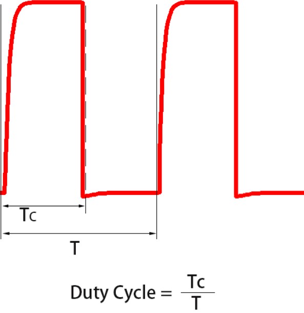
Astable Multivibrator Circuit Duty Cycle
It describes the proportion of time a signal is at a HIGH LEVEl within a complete cycle, typically used in the context of periodic or pulse signals. For example, if a signal is at a high level for 50% of the time in a cycle, then its “Duty Cycle” is 50%. This concept is very important in many electronic systems, including digital circuits, wireless communications, and audio processing.
In this case, when the transistor is in OFF status, its collector output HIGH LEVEL voltage, so,
Astable Multivibrator Circuit Calculator
Seconds
Seconds
V
V
V
mA
V
Please enter 0 if there is No Emitter Load
Why is the capacitor defined as 'discharging' even though the voltage at its negative plates is increasing?
The term “discharge” in this context is a bit counter-intuitive. When we say that the capacitor C1 is discharging, we mean that it is losing the charge it initially had. In the beginning, C1 is charged to the power supply voltage V with the polarity shown in the figure. This means that the left plate of C1 (connected to Q1) is positive, and the right plate (connected to Q2 base) is negative. When Q1 is turned on, it connects the left-hand positive plate of C1 to ground, effectively making it 0V. This causes the right-hand plate of C1 to be at a voltage of -V (since the voltage across the capacitor must be V). Now, C1 starts “discharging” through R2. But here’s the catch: the “discharge” of C1 is not the usual discharge process we think of where a charged capacitor releases its stored energy and goes towards 0V. Instead, because of the way the circuit is set up, the “discharge” of C1 actually involves the voltage at the right-hand plate of C1 (and at the base of Q2) rising from -V towards +V. So, even though the voltage at the right-hand plate of C1 is increasing, we still say C1 is discharging because it is losing the charge it initially had (with the left plate positive and the right plate negative). The increase in voltage at the right-hand plate of C1 is due to the current flowing through R2 from the positive supply, which reduces the magnitude of the negative charge at the right-hand plate of C1.Go Back[1]
Creative Commons tutorials are CC BY-SA 4.0 License